Advanced Search

ISSN1001-3806 CN51-1125/TN Map

Volume 43 Issue 6
Nov.  2019
Article Contents
Turn off MathJax

Citation:

Optimization of thin film solar cells with double-grating structure

  • Received Date: 2018-12-14
    Accepted Date: 2019-01-04
  • In order to improve the short circuit current density and conversion efficiency of crystalline silicon thin film solar cells, a silicon dielectric grating and an aluminium metal grating were integrated on the front and back of single crystal silicon thin film solar cells respectively. The effect of the period, thickness and duty cycle of both the gratings on the short-circuit current density and optical conversion efficiency of single crystal silicon thin film solar cells were simulated with finite difference time-domain software. The results show that, the short-circuit current density can reach 35.15mA/cm2 and the conversion efficiency is 43.35% when both the front and back gratings are at the optimum value (for the dielectric grating, duty cycle F=0.8, period P=0.632μm, thickness hg=0.42μm; for the metal grating, duty cycle F1=0.9, period P=0.632μm and thickness hm=0.005μm). After comparing the optimal grating monocrystalline silicon thin film solar cells with traditional monocrystalline silicon thin film solar cells, the grating monocrystalline silicon thin film solar cells have a significant improvement in both optical path and absorption efficiency. This study provides theoretical guidance for the preparation of high performance thin film solar cells in the future.
  • 加载中
  • [1]

    YAMAMOTO K, YOSHIMI M, SUZUKI T, et al. Thin film poly-Si solar cell on glass substrate fabricated at low temperature[J]. MRS Online Proceedings Library, 1998, 507(2):179-185.
    [2]

    SHAIK H, BASAVARAJU U, RACHITH S N, et al. Surface-plasmon-induced photoabsorption of Ag nanoparticle embedded a-Si solar cell[J]. Optical Materials, 2017, 73(3):179-187.
    [3]

    SHEN H J, LI T, LU H D, et al. Enhancement of light absorption in thin film silicon solar cells with light traping [J]. Chinese Journal of Luminescence, 2016, 37(7):816-822(in Chinese). doi: 10.3788/fgxb20163707.0816
    [4]

    MULLER J, RECH B, SPRINGER J, et al. TCO and light trapping in silicon thin film solar cells[J]. Solar Energy, 2004, 77(6):917-930. doi: 10.1016/j.solener.2004.03.015
    [5]

    SHI X, SUN Ch, WANG X Q. One-dimensional diffraction grating structure for rear reflection surface of thin film silicon solar cells[J]. Laser & Optoelectronics Progress, 2018, 55(1):010501 (in Chin-ese).
    [6]

    ZHU Zh P, QIN Y Q. Nanowires array designed by means of two-dimension closed-form solution for antireflection[J]. Acta Physica Sinica, 2013, 62(15):157801 (in Chinese).
    [7]

    JUNG S M, KIM Y H, KIM S I, et al. Design and fabrication of multi-layer antireflection coating for Ⅲ-Ⅴ solar cell[J]. Current A-pplied Physics, 2011, 11(3):538-541. doi: 10.1016/j.cap.2010.09.010
    [8]

    CATCHPOLE K R, POLMAN A. Design principles for particle plasmon enhanced solar cells[J]. Applied Physics Letters, 2008, 93(19):191113. doi: 10.1063/1.3021072
    [9]

    WANG K X, YU Z, LIU V, et al. Absorption enhancement in ultrathin crystalline silicon solar cells with antireflection and light-trapping nanocone gratings[J]. Nano Letters, 2012, 12(3):1616-1619. doi: 10.1021/nl204550q
    [10]

    GUPTA N D, JANYANI V, MATHEW M, et al. Light trapping in p-i-n superlattice based InGaN/GaN solar cells using photonic crystal [J]. Optical & Quantum Electronics, 2016, 48(11):1-17.
    [11]

    QIN F F, ZHANG H M, WANG C X, et al. Design and simulation of anodic aluminum oxide nanograting anti-reflection structure for thin film silicon solar cells[J]. Acta Physica Sinica, 2014, 63(19):198802(in Chinese).
    [12]

    SHAO G J. Investigation on the enhancement of conversion efficiency of solar cell [D]. Nanjing: Southeast University, 2016: 20-23(in Chinese).
    [13]

    ZHENG Z W, YU J, LAI M H, et al. Efficiency enhancement for resonant-cavity-enhanced InGaN/GaN multiple quantum well solar cells[J]. Vacuum, 2016, 12(1): 1-6.
    [14]

    IQBAL T, IJAZ M, JAVAID M, et al. An optimal au grating structure for light absorption in amorphous silicon thin film solar cell[J]. Plasmonics, 2018, 24(12):1-8.
    [15]

    HAKIM F, ALAM M K. Improvement of photo-current density of P3HT: PCBM bulk heterojunction organic solar cell using periodic nanostructures[C]// International Conference on Electrical, Computer and Communication Engineering. New York, USA: IEEE, 2017: 170-174.
    [16]

    ZHENG C G, JIANG J L, XIAN F L, et al. Design of periodic metal-insulator-metal waveguide back structures for the enhancement of light absorption in thin-film solar cells[J]. Chinese Physics, 2011, B20(9):192-197.
    [17]

    SCHUSTER C S, KOWALCZEWSKI P, MARTINS E R, et al. Dual gratings for enhanced light trapping in thin-film solar cells by a layer-transfer technique[J]. Optics Express, 2013, 21(9):A433-A438.
    [18]

    SHENG X Ch. Semiconductor spectroscopy and optical properties[M]. Beijing: Science Press, 2002:21-29(in Chinese).
    [19]

    YOU J, LI X, XIE F, et al. Surface plasmon and scattering-enhanced low-bandgap polymer solar cell by a metal grating back electrode[J]. Advanced Energy Materials, 2012, 2(10):1203-1207. doi: 10.1002/aenm.201200108
    [20]

    YABLONOVITCH E. Statistical ray optics[J]. Journal of the Optical Society of America, 1982, 72(7):899-907. doi: 10.1364/JOSA.72.000899
    [21]

    ULBRICH C, PETERS M, BLÄSI B, et al. Enhanced light trapping in thin-film solar cells by a directionally selective filter[J]. Optics Express, 2010, 18(s2):A133-A138. doi: 10.1364/OE.18.00A133
  • 加载中
通讯作者: 陈斌, bchen63@163.com
  • 1. 

    沈阳化工大学材料科学与工程学院 沈阳 110142

  1. 本站搜索
  2. 百度学术搜索
  3. 万方数据库搜索
  4. CNKI搜索

Figures(7)

Article views(6703) PDF downloads(15) Cited by()

Proportional views

Optimization of thin film solar cells with double-grating structure

  • College of Information Engineering, Quzhou College of Technology, Quzhou 324100, China

Abstract: In order to improve the short circuit current density and conversion efficiency of crystalline silicon thin film solar cells, a silicon dielectric grating and an aluminium metal grating were integrated on the front and back of single crystal silicon thin film solar cells respectively. The effect of the period, thickness and duty cycle of both the gratings on the short-circuit current density and optical conversion efficiency of single crystal silicon thin film solar cells were simulated with finite difference time-domain software. The results show that, the short-circuit current density can reach 35.15mA/cm2 and the conversion efficiency is 43.35% when both the front and back gratings are at the optimum value (for the dielectric grating, duty cycle F=0.8, period P=0.632μm, thickness hg=0.42μm; for the metal grating, duty cycle F1=0.9, period P=0.632μm and thickness hm=0.005μm). After comparing the optimal grating monocrystalline silicon thin film solar cells with traditional monocrystalline silicon thin film solar cells, the grating monocrystalline silicon thin film solar cells have a significant improvement in both optical path and absorption efficiency. This study provides theoretical guidance for the preparation of high performance thin film solar cells in the future.

引言
  • 在人类寻找的所有绿色能源当中,太阳能电池是最具有发展前景的一种能源,为了节约成本,近几年一些科学家提出利用薄膜太阳能电池(thin film solar cell, TFSC)发电[1-2]。但是虽然薄膜太阳能电池能够降低发电成本,不过由于其厚度减薄导致陷光能力下降,光电转换效率会大幅下降[3]

    为了提高薄膜太阳能电池的转换效率,不同科研团队采用了不同的方法,但所有这些方法最终目的是为了让更多的光子进入到太阳能电池吸收层[4],并增加这些光子在太阳能电池中的光程[5]。如在TFSC表面制绒[6]、增加减反层[7]、制备金属纳米颗粒或周期性光栅[8-9]、放置光子晶体或氧化铝纳米光栅[10-11]、添加YAG:Ce荧光粉[12]等都是为了增加入射太阳光在薄膜太阳能电池表面的透射;而在TFSC背面制备布喇格反射[13]、金属光栅[14]、周期性纳米阵列[15]、绝缘背反射波导结构[16]、加厚金属电极均是为了将没有被TFSC吸收层吸收的光反射回吸收层,从而提高光子在吸收层中的光程。

    为了提高单晶硅(C-Si)薄膜太阳能转换效率,作者在薄膜单晶硅的上表面制备由硅材料制备的周期性光栅和由氧化铟锡(indium tin oxides, ITO)材料制备的减反层,在薄膜的单晶硅背面制备了与硅光栅同周期的铝金属光栅,利用减反层和硅介质光栅对太阳光的增透性还有金属光栅的表面等离子体效应,不仅可以增加光子进入TFSC的数量, 还可以提高光子的光程,从而可以显著地提高单晶硅TFSC的转换效率。参考文献[17]中已经通过实验证明双光栅可以提高太阳能电池的吸收效率,但该文献中背面使用的还是介质硅光栅,并且没有计算出转换效率和短路电流密度。经过对单晶硅TFSC结构的设计和优化,最终可以使TFSC的短路电流密度JSC达到35.15mA/cm2,转换效率η理论上可以达到43.35%。

1.   薄膜太阳能电池结构设计
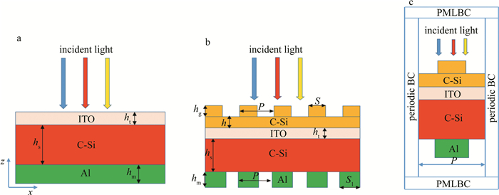
  • 图 1是单晶硅TFSC结构示意图。图 1a是传统单晶硅TFSC,它是由Al电极(厚度hm)、单晶硅吸收层(厚度hs)、减反层ITO(厚度ht)构成。图 1b是本文中提出的光栅单晶硅TFSC,它是在传统单晶硅TFSC的上下表面分别集成同周期的硅介质光栅和Al金属光栅。图中,h是硅介质光栅衬底厚度、hg是硅光栅厚度、P是上下表面光栅的周期、S是硅介质光栅条宽(介质光栅占空比F=S/P)、S1是Al金属光栅条宽(金属光栅占空比F1=S1/P)。图 1c是在利用有限时域差分法(finite difference time-domain, FDTD)模拟计算光栅单晶硅TFSC的短路电流密度和光转换效率时的计算单元。因为作者提出的光栅单晶硅TFSC是周期性结构,因此只需计算单晶硅TFSC的一个单元即可。在利用FDTD模拟中,在xz方向的边界上分别设置为周期性边界条件(periodic boundary condition, PBC)和完全匹配层边界条件(perfect matched layer boundary condition, PMLBC)。

    Figure 1.  Crystalline silicon TFSC structure diagram

2.   器件结构的优化
  • 太阳能电池其本质是一个将太阳光转换为电子空穴对的二极管,当太阳光照着在太阳能电池上时,相当于是在P-N结上添加了正向电压,此时太阳能电池的短路电流密度可由下式表示:

    式中, JSC是短路电流密度,J0是反向饱和电流密度,VOC是太阳能电池开了电压,k为常数,T为电池温度[18]

    另外, 太阳能电池的转换效率可利用电池的最大输出功率和入射光功率相除而得,由下式所示:

    式中,Pmax是电池最大输出功率,它是由电池开路电压VOC、电池短路电流密度和填充因子f决定; Pin是电池的外部入射功率,它是由太阳光入射光子流密度bin(λ)计算而得[12]λ是入射光波长。

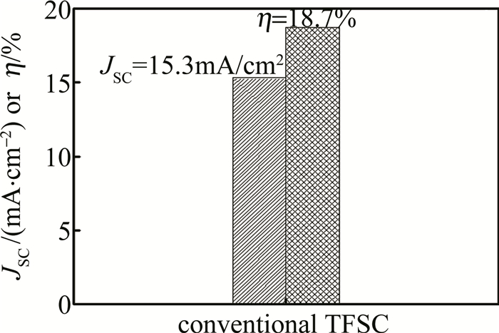
  • 图 2所示的是传统单晶硅TFSC的JSC(15.3mA/cm2)和η(18.7%)。图中得到的JSCη是在hs=0.4μm, hm=0.08μm, ht=0.02μm的条件下先利用FDTD计算出传统单晶硅TFSC的η,随后将η代入(2)式计算得到JSC。之所以传统单晶硅TFSC的JSCη相对较低是因为TFSC的吸收层仅有几百纳米,但是若想将长波长完全吸收,则要求吸收层厚度达到几十微米甚至几千微米,因此长波长的光将会透过吸收层而不被吸收,并且即使在薄膜表面由ITO之类的减反层[4],仍然有反射将太阳光反射回空气当中。

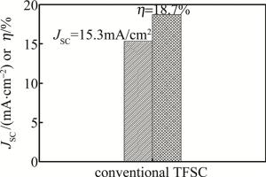
    Figure 2.  JSC and η of conventional crystal crystalline silicon TFSC

    为了能够提高传统单晶硅TFSC的短路电流密度和转换效率,本文中提出在传统单晶TFSC的上表面制备硅介质光栅,并且在下表面制备相同周期的Al金属光栅,结构如图 1b所示。Al金属光栅主要作用是利用其表面等离子体效应增加TFSC的背面反射,而硅介质光栅的作用是减少TFSC的表面反射,并且能够将从Al金属光栅反射回来的光又全反射进单晶硅吸收层内。

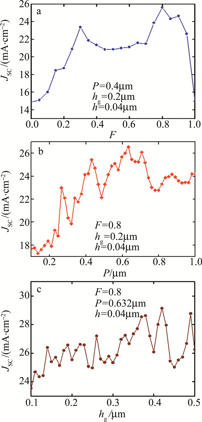
    图 3是当hs=0.4μm, hm=0.08μm, ht=0.02μm, h=0.04μm, F1=1时,表面硅介质光栅参量对光栅单晶硅TFSC短路电流密度的影响。从图 3中可以得到, 当介质光栅占空比F=0.8、光栅周期P=0.632μm、光栅厚度hg=0.42μm时,单晶硅TFSC的JSC可以达到29.13mA/cm2,相比于传统单晶硅TFSC的JSC提高了90.3%。

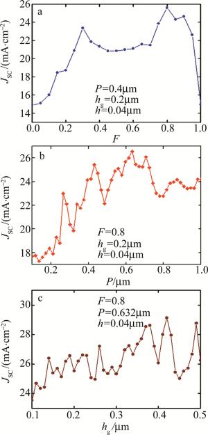
    Figure 3.  Influence of dielectric grating parameters on short circuit current density
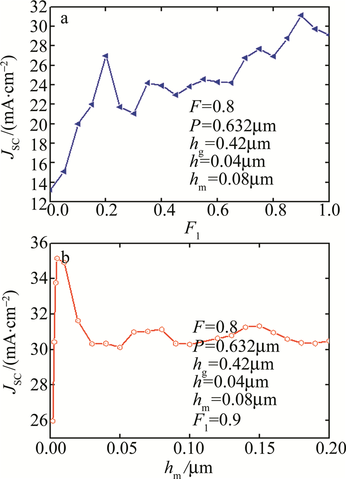
    图 4hs=0.4μm, ht=0.02μm, h=0.04μm, F=0.8, P=0.632μm, hg=0.42μm时,金属光栅参量对光栅单晶硅TFSC的短路电流密度的影响。通过图 4可以发现, 当F1=0.9,hm=0.005μm时,光栅单晶硅TFSC的短路电流密度可以达到35.15mA/cm2。虽然金属光栅(F1=0.9)厚度hm仅有0.005μm,但是在该参量下其实现的JSChm=0.08μm的金属(F1=1)高,之所以出现这种现象是因为太阳入射光波与Al金属光栅之间共振耦合形成表面等离子极化,使Al金属光栅与单晶硅交界面附近的电磁强度由于共振作用明显增强[19],从而使Al金属光栅对太阳光的反射高于厚度更高的金属层,最终提高了光栅单晶硅TFSC的JSC

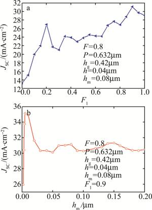
    Figure 4.  Influence of metal grating parameters on short circuit current density

3.   最优光栅单晶硅TFSC于传统单晶硅TFSC的对比
  • 提高光子在吸收层的光程是提高TFSC转换效率的关键问题之一,根据YABLONOVITCH计算得出,理论上最大光子光程[20]可由下式所示:

    式中, wopt(λ)是光子光程,L是光程路径提高因子,n是吸收层单晶硅的折射率。

    根据参考文献[21]可知,TFSC的反射率与光子在吸收层的光程和吸收层的吸收系数有关,如下式所示:

    式中, α(λ)为吸收层吸收系数,r(λ)为TFSC的反射率。

    根据(3)式和(4)式可知,光程路径提高因子可由下式表示:

    式中,Lc(λ)和Lg(λ)分别表示传统单晶硅TFSC路径提高因子和光栅单晶硅路径提高因子,rc(λ)和rg(λ)分别表示传统单晶硅TFSC的反射率和光栅单晶硅TFSC的反射率。

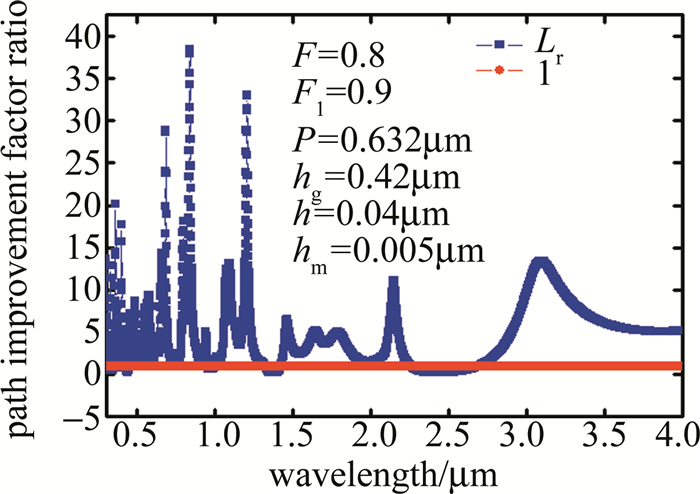
    (7) 式是光栅单晶硅TFSC与传统单晶硅TFSC光程路径提高因子的比值Lr,当Lr>1, 说明相同波长的光子在光栅单晶硅TFSC吸收层的光程路径相对于传统单晶硅TFSC有提高,当Lr < 1, 说明相同波长的光子在光栅单晶硅TFSC吸收层的光程路径相对于传统单晶硅TFSC有减小。

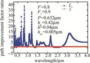
    Figure 5.  Lr values corresponding to different wavelengths

    图 5是不同波长对应的Lr值。从图中可以看见,当入射光波长从0.3μm增加到4μm的过程中,Lr几乎都是大于1,而且最大值可以达到40,仅有一小部分波段对应的Lr < 1。由此可知,通过优化后光栅单晶硅TFSC的光程路径有了显著的提高,因此才会使其JSC达到35.15mA/cm2

  • 衡量光栅单晶硅TFSC吸收效率相比于传统单晶硅TFSC是提高还是下降,本文中用吸收率增强因子Ae来表述,Ae的表达式如下式所示:

    式中, Ag(λ)和Ac(λ)分别是最优光栅单晶硅TFSC和传统单晶硅TFSC对应不同波长的吸收效率。当Ae>0,说明光栅单晶硅TFSC的吸收效率比传统单晶硅TFSC的高;而当Ae < 0,则说明光栅单晶硅TFSC的吸收效率比传统单晶硅TFSC的低。

    图 6是不同波长对应的吸收率增强因子Ae。从图中可以看到, 大部分的Ae均是大于0,并且最大值可以达到接近700%,只有在一部分波段内是Ae小于0,由此可以得出最优光栅单晶硅TFSC的吸收效率有了显著的提高。

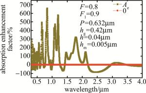
    Figure 6.  Ae values corresponding to different wavelengths

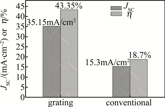
  • 图 7是由(1)式和(2)式计算得到的最优光栅单晶硅TFSC的短路电流密度和转换效率, 并将其与传统单晶硅的TFSC进行对比。从图中可以发现, 最优光栅单晶硅TFSC的JSCη分别达到35.15mA/cm2和43.35%,相比传统的有了明显的提高,在转换效率上, 最优单晶硅TFSC相对于传统单晶硅TFSC提高了126.4%。

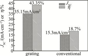
    Figure 7.  Comparison of JSC and η between optimal grating crystalline silicon TFSC and conventional crystalline silicon TFSC

4.   结论
  • 提出将硅介质光栅和Al金属光栅分别集成在传统单晶硅TFSC上下表面,利用FDTD方法研究了金属光栅参量和介质光栅参量对TFSC短路电流密度的影响,得出了最佳结构参量,当光栅周期P=0.632μm、介质光栅占空比F=0.8、介质光栅厚度hg=0.42μm、金属光栅占空比F1=0.9、金属光栅厚度hm=0.005μm时,光栅单晶硅TFSC在0.3μm~4μm的光谱范围内,短路电流密度JSC可达35.15mA/cm2,转换效率η可达43.35%。同时从TFSC的物理机制出发,对比了最优光栅单晶硅TFSC和传统单晶硅TFSC光程路径和吸收效率,从计算结果可知,无论是光程路径和吸收效率,最优光栅单晶硅TFSC都有显著的提高。

Reference (21)

Catalog

    /

    DownLoad:  Full-Size Img  PowerPoint
    Return
    Return