 网站地图
网站地图

 下载:
下载:


-
随着煤炭等传统能源的逐渐耗尽,亟需寻找一种新型、清洁、环保的能源。太阳能作为一种新型能源,取之不尽、用之不竭,如何高效利用太阳能成为广大研究者关注的焦点。无机半导体材料具有成本高、生产工艺复杂以及材料易腐蚀等特点,所以以无机半导体材料为原料的电池未能实现普及。与无机材料相比,有机半导体材料成本较低、光电性能优异,越来越受到广大科研工作者的青睐。
早在2004年,SUNDAR等人成功制备了有机小分子材料红荧烯单晶场效应晶体管[1]。2007年,LUO等人在超高真空的条件下,采用热蒸发的方法生长了红荧烯薄膜[2]。同年5月,PARK等人采用热蒸发的方法,通过控制衬底温度以及退火温度,制备了非晶及多晶的红荧烯薄膜[3]。2012年,DENG等人采用真空蒸镀的方法通过控制蒸镀时间制备了具有多晶结构的红荧烯薄膜[4]。异质结型有机太阳能电池由于成本低、柔韧性好等特点逐渐走进了广大科研工作者的视野。SHI等人利用化学气相沉积的方法成功地制备出石墨烯/二硫化钼异质结[5]。YU等人利用化学气相沉积的方法制备出MoS2,然后利用转移的方法同样制备大面积的石墨烯/二硫化钼异质结[6]。此外,基于MoS2/WS2异质结的光探测器开关比高于105,电子迁移率为65cm2·V-1·s-1,光响应高于1.42A·W-1[7]。异质结型有机太阳能电池存在载流子迁移率低、器件形貌不可有效调控和器件稳定性差等问题。作为一种有机小分子材料,8-羟基喹啉铝成膜性和热稳定性较好,并且具有较好的发光特性和电子传输特性因而显示出比较广阔的应用前景。
有机太阳能电池对薄膜性能的要求较高,载流子的特性十分重要,对影响载流子电输运特性的实验条件的要求也更加苛刻。本文中从温度、取样电阻及光脉冲能量三方面研究了对载流子迁移率的影响。
-
制备薄膜常用的方法有化学气相沉积法[8-10]和物理气相沉积法。LEE等人利用化学气相沉积的方法制备MoS2薄膜[11]。在沉积材料过程中,两种方法都需要合适的压力以及反应源,但相对化学气相沉积法而言,物理气相沉积法不需要反应源发生化学反应,不会产生副产物。本文中采用物理气相沉积的方法制备8-羟基喹啉铝(Alq3)本征薄膜[12]。首先将切割好的氧化铟锡(indium tin oxide, ITO)玻璃进行刻蚀与清洗,得到理想的ITO电极。由于不同衬底的温度会对薄膜产生不同影响[13], 作者利用DM-450A型镀膜机,采用物理气相沉积的方法在恒温条件下将粉末状Alq3在真空度为5mPa的高真空情况下蒸镀到刻蚀好的ITO电极上,在Alq3薄膜上蒸镀上需要的铝电极。至此,ITO/sample(Alq3)/Al电极这样类似三明治的Alq3本征薄膜制备完毕。
-
对已经蒸镀好的Alq3本征薄膜进行X射线衍射(X-ray diffraction, XRD)分析,得到如图 1所示的XRD曲线。
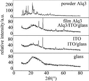
Figure 1. XRD for the samples of Alq3
热舟蒸镀法制备的Alq3薄膜与ITO电极的晶相结构差别不大,Alq3薄膜的衍射峰和ITO的衍射峰几乎出现在相同的衍射角上,说明样品薄膜中出现的两个峰即为ITO的峰,而薄膜的XRD曲线中除了ITO的峰以外没有出现其它尖峰,因此,认为Alq3薄膜是非晶态本征薄膜,满足实验要求。
-
本文中采用渡越时间(time-of-flight, TOF)方法对Alq3中载流子迁移率进行测量。该方法的电路原理如图 2所示。虚线框A中为蒸镀好的三明治式薄膜样品,其中厚度为L的Alq3薄膜两侧为电极,薄膜左侧为ITO电极,与电源负极相连接,右侧为Al电极,与电源正极相连接。R为取样电阻,包括外加电容C(积分电容)以及其它杂散电容在内的所有电容用虚线框B中的符号表示。外加直流电压为U,样品厚度为d。样品中有稳定的电场,其大小为:
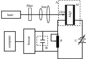
Figure 2. Circuit principle diagram of TOF method
$ {E_0} = \frac{U}{d} $
(1) 由于电源对样品的充电,ITO电极和Al电极上分别储存有一定的电荷,分别用-Q和+Q表示。当一个脉冲宽度小于载流子渡越时间的外激光脉冲照射到样品上时,光脉冲产生的载流子将在外电场作用下做宏观定向移动。t时间后距坐标原点的距离为x(取负极为坐标原点,水平向右为正方向)。由于静电感应现象的存在,t时刻,ITO电极上的总电荷为-Q+q1,Al电极上的总电荷为Q+q2(其中q1, q2为感应电荷)。由于感应电荷的出现,样品中的电场将以载流子层为分界层左右发生变化。假设载流子层左侧电场为$\vec E$l,右侧电场为$\vec E$r,由于电源电压不发生变化,因此:
$ {E_{\rm{l}}} \times x + {E_{\rm{r}}} \times \left( {d - x} \right) = {E_{\rm{0}}} \times d $
(2) 载流子生成之前,对Al电极应用高斯定理有:
$ S \cdot {\varepsilon _0}{\varepsilon _{\rm{r}}}{E_0} = Q $
(3) 式中,S为载流子层的面积;ε0和εr分别为真空电容率和样品的相对电容率。
载流子生成之后,对ITO电极和Al电极分别应用高斯定理有:
$ - S \cdot {\varepsilon _0}{\varepsilon _{\rm{r}}}{E_{\rm{l}}} = - Q + {q_1} $
(4) $ S \cdot {\varepsilon _0}{\varepsilon _{\rm{r}}}{E_{\rm{r}}} = Q + {q_2} $
(5) 联立方程(2)式~(5)式解得:
$ \left\{ \begin{array}{l} {q_1} = Ne\left( {1 - \frac{x}{d}} \right)\\ {q_2} = Ne\frac{x}{d} \end{array} \right. $
(6) $ \left\{ \begin{array}{l} {E_{\rm{l}}} = {E_0} - \frac{{Ne}}{{{\varepsilon _0}{\varepsilon _{\rm{r}}}S}}\left( {1 - \frac{x}{d}} \right)\\ {E_{\rm{r}}} = {E_0} + \frac{{Ne}}{{{\varepsilon _0}{\varepsilon _{\rm{r}}}S}} \cdot \frac{x}{d} \end{array} \right. $
(7) 式中,N为激励的总载流子数, e为电子电量。由于载流子在运动过程中受到深陷阱和浅陷阱的影响而不断损失,因此,N将不再保持不变。
ITO以及Al电极上的电荷会由于载流子层的运动而重新分布,当载流子层运动到位置x时,Al电极上的电荷变化量为:
$ \Delta Q = {\varepsilon _0}{\varepsilon _{\rm{r}}}S\Delta {E_{\rm{r}}} = \frac{{Nex}}{d} $
(8) 取样电阻两端电压相应发生变化:
$ \Delta U\left( t \right) = \frac{{Ne}}{{Cd}}x = \frac{{Ne}}{{Cd}}vt $
(9) 式中,v为载流子运动速率,t为时间, C为电容。
当tRCtTOF(其中,tRC为外电路的RC响应时间,tTOF为渡越时间)时,取样电阻上将会产生电流脉冲:
$ i = \frac{{Ne}}{d}v $
(10) 由电流脉冲测量出载流子运行时间,利用下式可计算出载流子的迁移率μ:
$ \mu = \frac{{{L^2}}}{{U{t_{{\rm{TOF}}}}}} $
(11) 然后讨论不同的实验条件对载流子迁移率的影响,给出测量载流子迁移率的最佳实验条件。
-
Scher-Montroll模型就是利用统计力学的概率性原理研究弥散输运中载流子的迁移率问题[15]。假设材料内部存在大量的规则晶胞,但这些晶胞的分布是随机的[16]。电荷的输运就是从一个晶胞到另一个晶胞的过程。由于晶胞的随机分布,载流子的移动速率将随机变化,以至于TOF信号会出现一个长长的尾巴[17]。SCHER和MONTROLL用跳跃时间的分布函数Ψ(t)≈cons(t-(1+α))来描述这种随机分布的影响, 其中α∈(0, 1)。由分布函数可见:α值越小,弥散输运的程度越高[18]。载流子在连续两个晶胞之间移动的平均距离用〈l〉表示,〈l〉∝tα,载流子移动形成的电流用下式表示:
$ I\left( t \right) \propto \left\{ \begin{array}{l} {t^{ - \left( {1 - \alpha } \right)}},\left( {\left\langle l \right\rangle < L} \right)\\ {t^{ - \left( {1 + \alpha } \right)}},\left( {\left\langle l \right\rangle \ge L} \right) \end{array} \right. $
(12) 式中,L表示样品薄膜的厚度,此即幂指数定律[19]。根据此式,采用对数坐标变换电流和时间坐标轴,就可以得到载流子的渡越时间。
-
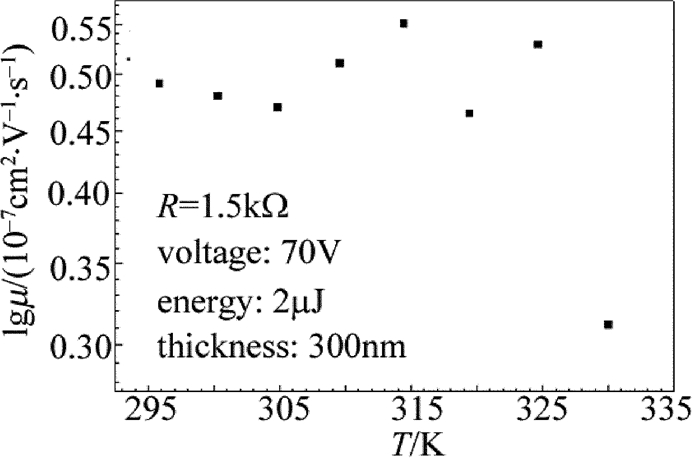
对于Alq3来说,取样电阻值设置为1.5kΩ,光脉冲能量为1.5μJ,外加电压为5V。图 3是Alq3样品中空穴的迁移率随温度的变化关系。
Figure 3. Relationship between mobility and temperature of the holes in Alq3
利用同样的方法测量了Alq3中电子的迁移率随温度的变化关系,见图 4。
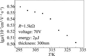
Figure 4. Relationship between mobility and temperature of the electrons in Alq3
从图 3和图 4可以看出:对于Alq3样品来说,其内部电子的迁移率在308K~338K的温度范围内与温度的关系满足线性关系,而其内部空穴的迁移率在同样的温度范围内波动较大,因此认为Alq3样品是良好的电子给体, 这与参考文献[20]中报道的基本一致。
-
TOF方法测量载流子迁移率的实验电路,相当于一个RC回路,其中取样电阻是电阻箱,而样品相当于一个平行板电容器,这样,实验的电路部分就构成了一个RC电路。TOF方法的一个基本实验条件即必须是小取样电阻,满足外电路的RC响应时间tRC小于载流子的寿命Tr,这样才能够保证测量的精度。图 5是Alq3中空穴的渡越时间与取样电阻的关系。用同样的方法得到了Alq3中电子的渡越时间与取样电阻的关系, 如图 6所示。
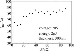
Figure 5. Relationship between tTOF and R of the holes in Alq3
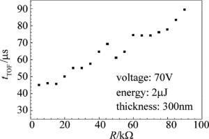
Figure 6. Relationship between tTOF and R of the electrons in Alq3
从图 5和图 6可以看出:对于Alq3样品,当取样电阻小于15kΩ时,样品内载流子的渡越时间基本处于恒定状态,在这个电阻范围内,载流子渡越时间基本不受取样电阻的影响。
-
TOF方法的另一个重要条件就是弱光注入,这样才不至于导致体激发。由于实验条件以及光脉冲能量的限制,实验过程中测量了光能量从1.5μJ~3.5μJ等不同光强时的渡越时间,得到了Alq3中电子载流子的渡越时间随光脉冲能量的变化关系,如图 7所示。
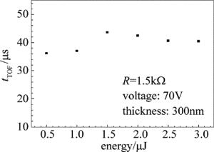
Figure 7. Relationship between tTOF and pulse energy of the electrons in Alq3
从图 7可以看出,当脉冲光的能量不大于3.5μJ时,Alq3中的光生载流子接近薄层分布,反映到渡越时间上就是渡越时间的值基本保持恒定,从而保证了测量的精度。
-
(1) 通过控制成膜条件,得到了Alq3样品薄膜,使得在308K~338K的温度范围内,Alq3中载流子输运规律符合浅陷阱模型。
(2) 测试电路的RC响应时间tRC<<Tr是保证测试结果准确性的前提条件。当取样电阻较大时,不能满足上述条件,就无法得到准确的飞行时间,进而对载流子的电输运特性造成影响;取样电阻较小时,采集到的信号比较微弱,此时,利用信号放大器放大信号并进一步得到有用信号,反映到渡越时间上,可以得到一个比较稳定的值。
(3) 光生载流子必须是薄层分布,因此弱光注入对本实验来说也非常重要。如果光能量太大,可能造成体激发,改变样品内部的电场,对载流子的电输运特性造成影响。
8-羟基喹啉铝本征薄膜的制备与性质研究
Preparation and study on characteristics of 8-hydroxy-quinoline aluminum film
-
摘要: 8-羟基喹啉铝属于有机半导体材料,在太阳能电池应用领域有较为广阔的应用前景。为了研究8-羟基喹啉铝载流子输运动力学信息,在恒温条件下制备了8-羟基喹啉铝薄膜,采用X射线衍射分析方法对薄膜的性质进行了分析,采用渡越时间方法对影响其载流子迁移率的实验条件进行了理论分析和实验验证。结果表明,在308K~338K温度范围内,8-羟基喹啉铝的载流子输运规律符合浅陷阱模型;取样电阻小于15kΩ及光脉冲能量低于3.5μJ时,载流子渡越时间保持恒定,测试结果可靠。这一结果对有机太阳能电池的制备是有帮助的。Abstract: 8-hydroxy quinoline aluminum is an organic semiconductor material and has broad application prospect in the field of solar cell application. In order to study the transport dynamic information of carriers, 8-hydroxyl quinoline aluminum thin film was prepared under the condition of constant temperature. The method of X-ray diffraction was used to analyze the properties of the film and the method of time-of-flight(TOF) was used to study the experimental conditions affecting the carrier mobility by theoretical analysis and experimental verification. The results show that this method is feasible. The carrier transport law of 8-hydroxy quinoline aluminum in the temperature range of 308K~338K is in accordance with shallow trap model. When the sampling resistance is less than 15kΩ and pulse energy is less than 3.5μJ, the carrier TOF remains constant. The test results are reliable. The result is helpful for the preparation of organic solar cells.
-
Key words:
- optoelectronics /
- transport dynamics /
- time-of-flight method /
- mobility
-
[1] SUNDAR V C, ZAUMSEIL J, PODZOROV V, et al. Elastomeric transistor stamps:reversible probing of charge transport in organic crystals[J]. Science, 2004, 303(5664):1644-1646. doi: 10.1126/science.1094196 [2] LUO Y, BRUN M, RANNOU P, et al. Growth of rubrene thin film, spherulites and nanowires on SiO2[J]. Physica Status Solidi, 2007, 204(6):1851-1855. doi: 10.1002/pssa.v204:6 [3] PARK S W, JEONG S H, CHOI J M, et al. Rubrene polycrystalline transistor channel achieved through in situ vacuum annealing[J]. Applied Physics Letters, 2007, 91(3):26-43. [4] DENG J X, KANG Ch L, YANG B, et al. Deposition and characterization of vacuum evaporated Rubrene films[J]. Chinese Journal of Vacuum Science and Technology, 2012, 32(8):678-681(in Ch-inese). [5] SHI Y M, ZHOU W, LU A Y, et al. Van der waals epitaxy of MoS2 layers using grapheme as growth templates[J]. Nano Letters, 2012, 12(6):2784-2791. doi: 10.1021/nl204562j [6] YU L L, HAN W, LEE Y H, et al. Graphene/MoS2 hybrid technology for large-scale two-dimensional electronics[J]. Nano Letters, 2014, 14(6):3055-3063. doi: 10.1021/nl404795z [7] HUO N J, KANG J, WEI Zh M, et al. Novel and enhanced optoelectronic performances of multilayer MoS2-WS2 heterostructure transistors[J]. Advanced Functional Materials, 2014, 24(44):7025-7031. doi: 10.1002/adfm.201401504 [8] CHEN Y Q, ZHANG Ch T, ZHANG J H. Simulation of temperature field of graphene substrate fabricated by laser chemical vapor deposition[J]. Laser Technology, 2015, 39(5):648-653(in Chinese). [9] HOU Zh J, TANG X, LUO M W, et al. Study on laser-induced chemical liquid deposition Fe film[J]. Laser Technology, 2016, 40(1):136-140(in Chinese). [10] ZHANG N, ZHOU B Q, ZHANG L R, et al. Research of hot wire chemical vapor deposition and micro-structure of a-SiNx: H thin film[J]. Laser Technology, 2016, 40(3):413-416(in Chinese). [11] LEE Y H, ZHANG X Q, ZHANG W J, et al. Synthesis of large-area MoS2 atomic layers with chemical vapor deposition[J]. Advanced Materials, 2012, 24(17):2320-2325. doi: 10.1002/adma.201104798 [12] SHI G, MEI L, GAO J S, et al. DUV LaF3 thin film deposited by IBS, thermal boat and electron beam evaporation[J]. Laser Technology, 2013, 37(5):592-595(in Chinese). [13] JIA F, CAO P J, ZENG Y X. Effect of substrate temperature on the properties of ZnO prepared with pulsed laser deposition method[J]. Laser Technology, 2010, 34(3):357-359(in Chinese). [14] LIU Q H, ZHANG Z H, LIU Zh Ch, et al. Study on measurement method of carrier mobility in weak photoconductive material[J]. Laser Technology, 2014, 38(4):445-448(in Chinese). [15] HUANG Ch H, LI F Y, HUANG Y Y. Optoelectronic functional ultrathin films[M]. Beijing:Peking University Press, 2004:238-298(in Chinese). [16] SCHER H, ELLIOTT W, MONTROL L. Anomalous transit-time dispersion in amorphous solids[J]. Physical Review, 1975, B12(6):2455-2477. [17] WU F, TIAN W J, ZHANG Zh M, et al. Organic electioluminescent device based on balanced carriers injection and transportation[J]. Thin Solid Films, 2000, 363(1):214-217. [18] BASSLER H. Hopping conduction in polymers[J]. International Journal of Modern Physics, 1994, B8(7):847-854. [19] FORERO S, NGUYEN P H, BRUTTING W, et al. Charge carrier transport in poly(p-phenylenevinylene) light-emiting devices[J]. Physical Chemistry Chemical Physics, 1999, 1(8):1769-1776. doi: 10.1039/a808614a [20] LIN P, LIANG Ch J, DENG Zh B, et al. Photovoltaic character of organic el devices MEH-PPV/Alq3[J]. Spectroscopy and Spectral Analysis, 2005, 25(1):23-25(in Chinese). -

 点击查看大图

图(7)
计量
- 文章访问数: 4149
- HTML全文浏览量: 2442
- PDF下载量: 281
- 被引次数: 0
